

- English
 Español
 Português
 русский
 Français
 日本語
日本語 Deutsch
 tiếng Việt
 Italiano
 Nederlands
 ภาษาไทย
 Polski
 한국어
한국어 Svenska
 magyar
 Malay
Malay বাংলা ভাষার
 Dansk
Dansk Suomi
Suomi हिन्दी
 Pilipino
 Türkçe
 Gaeilge
 العربية
 Indonesia
 Norsk
Norsk تمل
تمل český
český ελληνικά
 український
 Javanese
 فارسی
فارسی தமிழ்
தமிழ் తెలుగు
 नेपाली
 Burmese
 български
 ລາວ
ລາວ Latine
 Қазақша
 Euskal
 Azərbaycan
 Slovenský jazyk
 Македонски
 Lietuvos
 Eesti Keel
 Română
 Slovenski

What is the True Impact of 5G on Your Consumer Electronic PCBA and How Can You Prepare for It
Hello and welcome. Over my 20 years working closely with technology innovators, I have seen waves of change, from the dawn of Wi-Fi to the Internet of Things. But few technologies carry the transformative weight—and the hidden complexities—of 5G. Everyone talks about blazing-fast speeds and low latency, but what does this truly mean for the heart of your device, the Consumer Electronic PCBA? At Greeting, we have spent countless hours in our labs and on production floors, not just anticipating these changes but mastering them. This article isn't just theory; it's a practical guide born from hands-on experience, designed to help you navigate the fundamental shifts 5G imposes on Consumer Electronic PCBA design and manufacturing.
How Does 5G Fundamentally Reshape the Core of Consumer Electronic PCBA Design
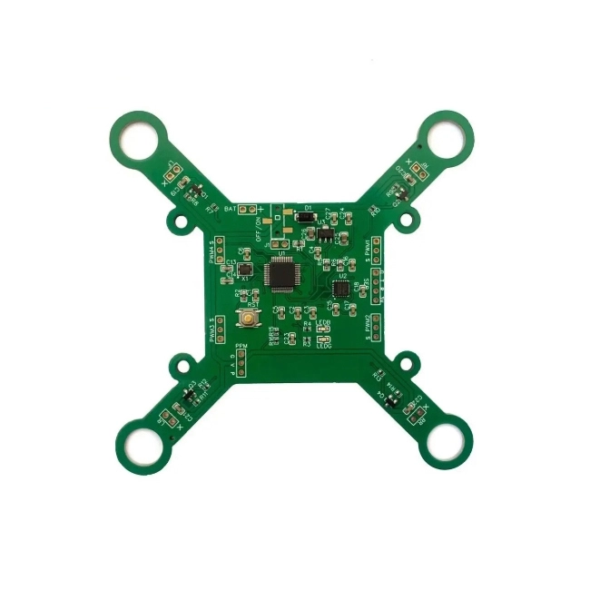
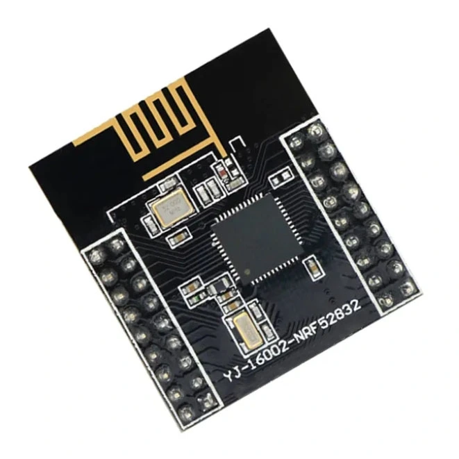
The leap to 5G is not a simple incremental upgrade. It's a paradigm shift that strikes at the very foundation of printed circuit board assembly. The move to higher frequency bands, like mmWave, transforms the Consumer Electronic PCBA from a simple electronic interconnect into a high-frequency signal pathway where every millimeter matters. The three primary battlegrounds we see are signal integrity, thermal management, and component density.
First, signal integrity is paramount. At multi-gigahertz frequencies, a PCB laminate that worked perfectly for 4G can become a source of significant signal loss. The Consumer Electronic PCBA must be treated as a waveguide, requiring materials with a stable and low dielectric constant (Dk) and an exceptionally low dissipation factor (Df). Impedance control is no longer a suggestion; it is an absolute necessity, with tolerances becoming dramatically tighter. Second, the increased data throughput and processing power generate concentrated heat. Effective thermal management is no longer about adding a heatsink as an afterthought; it must be engineered into the Consumer Electronic PCBA layout from the first schematic capture, using thermal vias, advanced substrates, and strategic component placement. Finally, the demand for smaller, more powerful devices pushes us towards High-Density Interconnect (HDI) technologies. This means finer traces, micro-vias, and a level of precision that separates a functional prototype from a reliable, mass-producible product.
What Key Parameters Define a Truly 5G-Ready Consumer Electronic PCBA
So, what should you look for when specifying your next board? It comes down to measurable, non-negotiable parameters. At Greeting, we have moved beyond standard FR-4 materials for these applications. The table below illustrates the stark contrast between a conventional approach and the specialized engineering required for a robust 5G Consumer Electronic PCBA.
Table 1: Critical Parameter Comparison for 5G Applications
| Key Parameter | Standard Consumer Electronic PCBA | Greeting's 5G-Optimized PCBA |
|---|---|---|
| Laminate Material | Standard FR-4 | High-frequency laminates (e.g., Rogers, Taconic) |
| Dissipation Factor (Df) | ~0.02 | ≤ 0.004 |
| Impedance Control Tolerance | ±10% | ±5% or tighter |
| Thermal Conductivity | ~0.3 W/m/K | > 0.5 W/m/K |
| Minimum Trace/Space | 4/4 mil | 2/2 mil (HDI capable) |
| Preferred Surface Finish | HASL, ENIG | ENIG or ENEPIG for superior RF performance |
Let's break down why these parameters are critical. A lower Dissipation Factor (Df) directly translates to less signal loss, ensuring the power your device transmits actually reaches the antenna effectively. Tighter impedance control prevents signal reflections that can corrupt data and degrade connection quality. The enhanced thermal conductivity of our chosen materials helps dissipate heat from powerful 5G modems and processors, preventing thermal throttling and ensuring long-term reliability. These are not just numbers on a datasheet; they are the bedrock of a high-performance Consumer Electronic PCBA that will not become the weakest link in your 5G product.
Consumer Electronic PCBA FAQ – Your Top Questions Answered Directly from Our Engineering Floor
In our conversations with clients, certain questions arise time and again. Here are the three most common ones, answered with the detail you deserve.
What is the single biggest oversight you see in early 5G Consumer Electronic PCBA designs
The most common mistake is underestimating the interplay between the laminate material and the power amplifier (PA). Designers often select a standard material to control costs, but this leads to excessive heat generation and signal loss at 5G frequencies. This forces the PA to work harder, creating a vicious cycle of heat and inefficiency. Investing in the right high-frequency laminate from the start is actually the most cost-effective choice, as it avoids performance issues and redesigns later.
How does Greeting specifically ensure signal integrity across the entire board
Our process is built on prevention, not correction. We employ advanced electromagnetic simulation software during the design phase to model signal paths and identify potential integrity issues before a single board is fabricated. Furthermore, we maintain a stringent controlled impedance fabrication process, with continuous monitoring and testing using Time Domain Reflectometry (TDR) on production panels. This end-to-end focus on the signal path is what defines our Consumer Electronic PCBA quality.
Can your platform support the full turnkey needs of a complex, high-volume 5G product
Absolutely. This is where our integrated model shines. We manage the entire journey: from initial Design for Manufacturability (DFM) analysis and component sourcing from our vetted, franchised distributors to precision manufacturing and rigorous final testing. We understand the supply chain challenges associated with advanced components and have the relationships and logistics expertise to ensure your project stays on schedule.
How Do We Validate and Certify the Performance of a 5G-Optimized Consumer Electronic PCBA
Designing to a spec is one thing; proving it in practice is another. Our validation protocol is exhaustive, leaving no room for uncertainty. We subject every batch of 5G-focused Consumer Electronic PCBA to a battery of tests that simulate the real-world demands your product will face over its lifetime.
Table 2: Our Comprehensive Consumer Electronic PCBA Validation Protocol
| Test Category | Specific Tests Performed | Performance Standard |
|---|---|---|
| Signal Integrity (RF Testing) | S-parameters (Insertion Loss, Return Loss), Vector Network Analyzer (VNA) | Meets or exceeds datasheet specs for all active components |
| Thermal Reliability | Thermal Cycling (-40°C to +125°C), Highly Accelerated Life Test (HALT) | No failures after 1000 cycles; stable performance under extreme stress |
| Functional & Electrical | In-Circuit Test (ICT), Flying Probe Test, Power-On Test | 100% electrical connectivity and basic functional verification |
| Long-Term Durability | Vibration Test, Mechanical Shock Test | Validates solder joint integrity and structural robustness |
This rigorous process ensures that when we deliver your Consumer Electronic PCBA, it is not just a collection of well-placed components. It is a validated, reliable subsystem that you can integrate into your product with confidence. This level of diligence is what transforms a potential product failure into a market success.
Are You Ready to Bridge the Gap Between 5G Ambition and Reliable Hardware Reality
The promise of 5G is real, but it is built on the foundation of a meticulously engineered Consumer Electronic PCBA. The challenges of signal loss, heat, and density are significant, but they are not insurmountable. They simply require a manufacturing partner who has already invested in the expertise, materials, and validation processes to turn these challenges into your competitive advantage. At Greeting, we have built our reputation on this exact principle. We don't just assemble boards; we engineer solutions for the connected future. The question is no longer what the impact of 5G is, but how you will successfully harness it.
Don't let Consumer Electronic PCBA complexities be the bottleneck that delays your next breakthrough. Contact us today for a confidential consultation. Let our experts review your design files, provide a detailed DFM analysis, and give you a clear path forward. Contact us now and let's build the future, together.
Send Inquiry


X
We use cookies to offer you a better browsing experience, analyze site traffic and personalize content. By using this site, you agree to our use of cookies.
Privacy Policy