

- English
 Español
 Português
 русский
 Français
 日本語
日本語 Deutsch
 tiếng Việt
 Italiano
 Nederlands
 ภาษาไทย
 Polski
 한국어
한국어 Svenska
 magyar
 Malay
Malay বাংলা ভাষার
 Dansk
Dansk Suomi
Suomi हिन्दी
 Pilipino
 Türkçe
 Gaeilge
 العربية
 Indonesia
 Norsk
Norsk تمل
تمل český
český ελληνικά
 український
 Javanese
 فارسی
فارسی தமிழ்
தமிழ் తెలుగు
 नेपाली
 Burmese
 български
 ລາວ
ລາວ Latine
 Қазақша
 Euskal
 Azərbaycan
 Slovenský jazyk
 Македонски
 Lietuvos
 Eesti Keel
 Română
 Slovenski

How Does PCB Cloning Differ from PCB Reverse Engineering?
In the world of electronics, Printed Circuit Boards (PCBs) are crucial for the functionality of various devices. When there is a need to replicate, analyze, or improve an existing PCB, two common methods come into play: PCB cloning and PCB reverse engineering. While they may seem similar, they serve different purposes and involve distinct processes. Understanding the differences between these two techniques can help determine which approach is best suited for a particular project.
What is PCB Cloning?
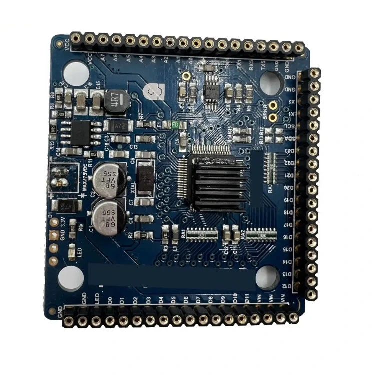
PCB cloning is the process of duplicating an existing PCB without making any modifications. This method is often used when the original design files, such as schematics and Gerber files, are unavailable but a working replica of the board is needed.
The cloning process begins by analyzing the physical PCB, scanning its layers, and extracting the layout and circuit traces. Advanced software tools help replicate the PCB’s design, including the placement of electronic components and copper traces. Once the data is gathered, a new board is manufactured to be an exact copy of the original.
PCB cloning is commonly used for replacing obsolete or discontinued PCBs, producing identical copies for large-scale manufacturing, and recovering lost designs. Since this method focuses on replication rather than redesign, it does not involve any performance enhancements or circuit modifications.
What is PCB Reverse Engineering?
PCB reverse engineering is a more detailed and analytical approach that involves studying the PCB’s design to understand how it functions. This technique is often used to troubleshoot issues, improve existing designs, or recreate schematics for a PCB that lacks documentation.
Unlike cloning, reverse engineering does not simply copy the PCB; instead, it breaks down the circuit design, traces signal paths, and identifies how components interact. Engineers may disassemble the board layer by layer, map out connections, and reconstruct the original schematics. This process allows for modifications, such as replacing outdated components, optimizing the circuit for better performance, or redesigning the board for specific improvements.
PCB reverse engineering is widely used in product development, failure analysis, research and development, and upgrading old electronic systems. It is an essential tool for engineers looking to enhance or modify an existing PCB rather than just duplicating it.
Key Differences Between PCB Cloning and PCB Reverse Engineering
The fundamental difference between PCB cloning and PCB reverse engineering lies in their purpose and complexity. Cloning focuses on making an exact duplicate without changes, while reverse engineering involves detailed analysis and possible modifications to the design.
PCB cloning is ideal when the goal is to reproduce an existing board as it is, whether for manufacturing, repair, or replacing outdated components. In contrast, reverse engineering is the preferred approach when improvements, troubleshooting, or design recovery are needed.
While both techniques are valuable in electronics, choosing the right method depends on the specific needs of the project. If you need an exact replica, PCB cloning is the way to go. If you need insights into the design and potential improvements, PCB reverse engineering is the better option.
In the field of PCB Clone, Greeting, as a leader, has always been imitated but never surpassed. The company combines the latest EDA design software, professional copying technicians and advanced process technology to clone single-layer, double-layer, multi-layer (up to 48 layers) PCB circuit boards, and can copy various high-difficulty PCB circuit boards such as blind and buried holes.Visit our website at www.grtpcba.com to learn more about our products. For inquiries, you can reach us at sales666@grtpcba.com.
Previous:Consumer Electronic PCBA Maintenance
Send Inquiry


X
We use cookies to offer you a better browsing experience, analyze site traffic and personalize content. By using this site, you agree to our use of cookies.
Privacy Policy