

- English
 Español
 Português
 русский
 Français
 日本語
 Deutsch
 tiếng Việt
 Italiano
 Nederlands
 ภาษาไทย
 Polski
 한국어
 Svenska
 magyar
 Malay
 বাংলা ভাষার
 Dansk
 Suomi
 हिन्दी
 Pilipino
 Türkçe
 Gaeilge
 العربية
 Indonesia
 Norsk
 تمل
 český
 ελληνικά
 український
 Javanese
 فارسی
 தமிழ்
 తెలుగు
 नेपाली
 Burmese
 български
 ລາວ
 Latine
 Қазақша
 Euskal
 Azərbaycan
 Slovenský jazyk
 Македонски
 Lietuvos
 Eesti Keel
 Română
 Slovenski

How Does a Single-Sided Thermoelectric Separation Copper Substrate Improve Heat Dissipation and PCB Reliability
As electronic devices continue to deliver higher power output in increasingly compact designs, effective thermal management has become a critical factor in PCB engineering. A Single-sided thermoelectric separation copper substrate provides an advanced solution by separating electrical circuit paths from dedicated heat conduction paths, helping electronic components transfer heat more efficiently while maintaining reliable electrical insulation. Greeting, a professional PCB and PCBA manufacturer, provides customized copper substrate solutions designed to meet demanding thermal management, structural precision, and electrical performance requirements across different industries. By combining high-quality copper materials with advanced manufacturing processes, Greeting supports electronic manufacturers seeking dependable thermal management solutions for high-power applications.
A single-sided thermoelectric separation copper substrate is a specialized metal-based printed circuit board designed to improve heat transfer by separating thermal conduction areas from electrical circuit structures. Unlike conventional PCB designs that rely on heat passing through an insulating layer, this structure can provide a more direct thermal pathway between heat-generating components and the copper base. This article explains its working principles, structural characteristics, manufacturing considerations, advantages, applications, and selection criteria. It also explores how Greeting's customized manufacturing capabilities can help engineers develop reliable thermal management solutions for demanding electronic products.
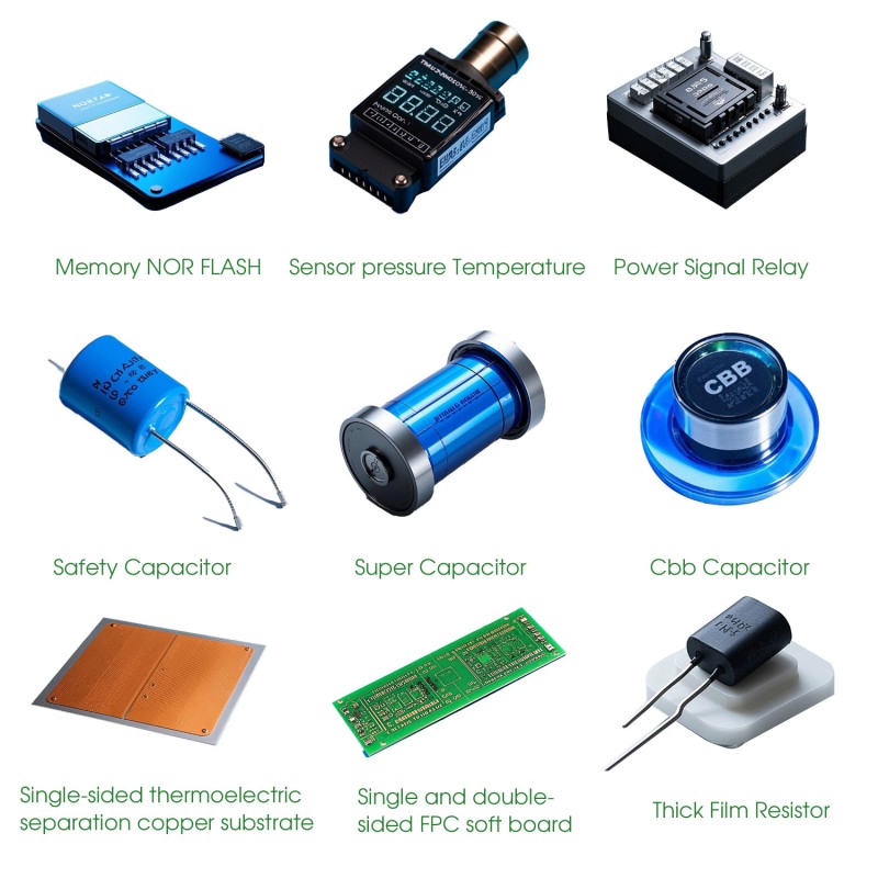
Table of Contents
- What Is a Single-Sided Thermoelectric Separation Copper Substrate?
- How Does Thermoelectric Separation Technology Work?
- Key Structural Features and Material Characteristics
- Technical Specifications and Manufacturing Capabilities
- What Are the Main Advantages?
- Typical Industrial Applications
- Comparison with Conventional PCB Substrates
- How to Select the Right Copper Substrate
- Manufacturing Quality and Reliability Control
- Frequently Asked Questions
- Conclusion: Choosing a Reliable Manufacturing Partner
1. What Is a Single-Sided Thermoelectric Separation Copper Substrate?
A Single-sided thermoelectric separation copper substrate is a specialized PCB structure that separates the electrical conduction area from the thermal conduction area. It is particularly suitable for electronic assemblies where concentrated heat generation creates challenges for conventional circuit board structures.
Traditional metal-based PCBs generally consist of three basic layers:
- Circuit layer: Copper foil used to establish electrical connections between electronic components.
- Insulation layer: A dielectric material that electrically isolates the circuit from the metal base while allowing heat transfer.
- Metal substrate: An aluminum or copper base that provides mechanical support and helps distribute heat.
In a thermoelectric separation structure, dedicated thermal contact regions are designed to establish a more direct heat transfer route to the metal base. This reduces the dependence on the conventional dielectric thermal pathway in designated heat dissipation areas.
The term single-sided generally describes the circuit-side configuration. The exact structure, number of internal layers, thermal contact geometry, and insulation arrangement should be confirmed according to the engineering drawing and manufacturing requirements.
For high-power electronic products, this technology offers an alternative to conventional thermal management structures where component temperature and board reliability are major design concerns.
2. How Does Thermoelectric Separation Technology Work?
The primary purpose of thermoelectric separation is to establish independent electrical and thermal pathways within a PCB structure. This arrangement allows heat generated by electronic components to reach the copper substrate through designated thermal contact regions without compromising the required electrical isolation.
Electrical and Thermal Path Separation
During operation, power components generate heat as electrical energy is converted into useful output and thermal losses. If this heat accumulates around the component, it may accelerate material aging, increase operating temperatures, and reduce product reliability.
A thermoelectric separation copper substrate addresses this challenge through several structural design principles:
- Dedicated thermal contact areas: Thermal contact regions are designed beneath or near heat-generating components.
- Independent circuit layout: Electrical copper patterns are arranged to maintain the required insulation distances.
- Direct heat transfer: Designated thermal contact structures connect the heat source more directly to the copper base.
- Heat spreading: The copper substrate distributes transferred heat toward the available cooling area.
- External heat dissipation: Heat can subsequently be transferred to a heatsink, housing, or surrounding environment.
Why Is This Structure Important?
The main advantage is the reduction of thermal resistance along the intended heat transfer path. However, actual performance depends on contact geometry, material properties, interface quality, component power, and the external cooling system.
Engineers should therefore evaluate the complete thermal design rather than relying on copper conductivity alone.
3. Key Structural Features and Material Characteristics
The performance of a thermoelectric separation PCB depends on the interaction between its copper base, circuit structure, insulation materials, and thermal contact regions.
High-Purity Copper Base
Copper is widely used in high-performance thermal management applications because of its excellent thermal conductivity and electrical conductivity. Its mechanical strength and structural stability also make it suitable for precision PCB manufacturing.
Compared with conventional aluminum-based substrates, copper-based structures can provide different advantages in thermal spreading, current-carrying design, and component integration. Material selection should be based on the actual thermal and mechanical requirements.
Thermal and Electrical Isolation Design
Separating the heat conduction path from the electrical circuit path is essential. The insulating materials and geometric clearances must be carefully selected to meet the required operating voltage, temperature, and safety standards.
Customized Board Geometry
Different electronic products require different thermal contact structures. Depending on the application, the design may include copper protrusions, recessed regions, or customized thermal contact arrangements.
These structures help engineers adapt the board to component packaging requirements and available installation space.
4. Technical Specifications and Manufacturing Capabilities
Manufacturing flexibility is an important consideration when selecting a copper substrate supplier. Greeting provides a range of customization options for thermoelectric separation copper substrates, allowing customers to specify board dimensions, copper thickness, structural configurations, and other production requirements.
The following table summarizes the published product specifications:
| Technical Parameter | Published Specification |
|---|---|
| Product Type | Single-sided Thermoelectric Separation Copper Substrate |
| Copper Thickness | 0.5–20 oz, maximum 33 oz |
| Minimum Aperture | 0.08 mm |
| Minimum Line Spacing | 2 mil |
| Board Thickness | 0.1–7 mm |
| Number of Layers | 1–40 layers |
| HDI Construction | Any layer, up to 4+N+4 |
| Surface Treatment | Bare copper, lead-free soldering, gold plating, and other options |
| Flammability Rating | UL 94V-0 |
| V-CUT Tolerance | ±10 mil |
| Maximum Warpage and Deformation | ≤0.50% |
| Quality Inspection | AOI and 100% electrical testing |
Engineering note: These are published manufacturing specifications, not a guarantee that every parameter can be achieved simultaneously in every design. Final capabilities, tolerances, and inspection criteria should be confirmed with Greeting before production.
Customization Options
For different PCB projects, customers may discuss the following requirements:
- Customized substrate dimensions and board thickness.
- Different copper weight requirements according to current loading.
- Thermoelectric separation layer configuration.
- Customized thermal contact areas and copper structures.
- Surface finishing options based on soldering and assembly needs.
- Special drilling, routing, and outline requirements.
5. What Are the Main Advantages of a Single-Sided Thermoelectric Separation Copper Substrate?
Choosing the right substrate structure can influence thermal performance, component operating conditions, product dimensions, and long-term reliability. A single-sided thermoelectric separation copper substrate offers several important engineering benefits.
1. More Efficient Heat Transfer
The most significant benefit is the ability to create a more direct thermal pathway between selected electronic components and the copper base. Reducing unnecessary thermal barriers can help lower the thermal resistance of the component-to-substrate interface.
2. Improved Thermal Management for High-Power Components
High-power LEDs, power semiconductor devices, and other heat-generating components require stable operating temperatures. A dedicated thermal pathway helps manage localized heat concentrations and supports more consistent operating conditions.
3. Better Electrical Insulation Design
Separating thermal contact regions from electrical circuit patterns allows engineers to optimize the thermal and electrical structures independently. Appropriate dielectric materials and clearances remain essential for electrical safety.
4. Compact Product Integration
Effective heat transfer can provide greater flexibility when designing compact electronic assemblies. Depending on the cooling requirements, engineers may be able to optimize heatsink dimensions, component spacing, and PCB layout.
5. Flexible Manufacturing Customization
Different products have different thermal loads, operating voltages, and mechanical limitations. Greeting's customization capabilities help customers develop substrate configurations according to their project drawings and application requirements.
6. What Are the Typical Applications of Thermoelectric Separation Copper Substrates?
Thermoelectric separation technology is particularly relevant to applications where electronic components generate concentrated heat and require reliable thermal management.
High-Power LED Lighting
LED modules convert part of their electrical input into heat. Excessive junction temperatures can affect luminous output, color stability, and component service life. A copper substrate with a dedicated thermal pathway can help transfer heat away from LED packages.
Automotive Electronics
Automotive electronic systems often operate under demanding temperature and vibration conditions. Power control modules, lighting systems, and other electronic assemblies may benefit from carefully engineered copper substrate structures.
Power Electronics
Power conversion equipment, switching circuits, and semiconductor modules can generate substantial localized heat. Thermoelectric separation structures provide another design option for managing thermal loads in these applications.
Industrial Control Equipment
Industrial control products frequently require continuous operation and dependable electrical performance. Improved thermal management can help maintain stable operating conditions in compact control assemblies.
Communication and Electronic Equipment
High-density electronic systems may contain components with significant power dissipation requirements. Proper substrate selection helps engineers balance thermal performance, electrical insulation, and mechanical integration.
Typical application areas include:
- High-brightness LED modules.
- Automotive lighting and power control systems.
- Industrial power supplies.
- Power semiconductor assemblies.
- Electronic control modules.
- High-power communication equipment.
7. How Does It Compare with Conventional PCB Substrates?
Different PCB substrate technologies offer different combinations of thermal conductivity, electrical insulation, manufacturing complexity, and cost. Understanding these differences helps engineers select the appropriate structure.
| Comparison Factor | FR-4 PCB | Aluminum Substrate | Thermoelectric Separation Copper Substrate |
|---|---|---|---|
| Base Material | Glass-fiber epoxy | Aluminum | Copper |
| Thermal Management | Limited by conventional PCB construction | Suitable for many thermal applications | Designed for more direct thermal transfer in designated areas |
| Electrical Insulation | Provided by FR-4 material | Provided by dielectric layer | Provided by the engineered insulation structure |
| Thermal Contact Design | Typically uses vias and other thermal features | Generally transfers heat through the dielectric layer | Uses dedicated thermal contact structures |
| Typical Applications | General electronic circuits | LED lighting and power electronics | High-power and concentrated heat-source applications |
| Manufacturing Complexity | Generally lower | Moderate | Higher due to specialized structural processing |
It is important to understand that thermoelectric separation copper substrates are not automatically the best choice for every PCB project. FR-4 remains suitable for many standard electronic applications, while aluminum substrates can provide a cost-effective solution for numerous thermal management requirements.
The separation copper structure becomes particularly attractive when the application requires a dedicated thermal connection that conventional metal-based PCB constructions cannot easily provide.
8. How to Select the Right Single-Sided Thermoelectric Separation Copper Substrate?
Selecting a suitable substrate requires more than comparing copper thickness or board dimensions. Engineers should evaluate the entire electronic assembly, including component heat generation, electrical insulation, mechanical structure, and cooling conditions.
Step 1: Evaluate Thermal Requirements
Determine the power dissipation of the heat-generating components and identify the maximum allowable operating temperature. Thermal simulation or prototype testing can help verify whether the proposed structure meets the requirements.
Step 2: Confirm Electrical Parameters
Specify operating voltage, current, insulation requirements, clearance distances, and circuit spacing. These factors directly influence the PCB layout and insulation material selection.
Step 3: Select Copper Thickness
Copper thickness should match current-carrying requirements and manufacturing constraints. Higher copper weight may improve electrical current capacity, but it also affects etching, dimensional accuracy, and production complexity.
Step 4: Review Mechanical Dimensions
Confirm board thickness, overall dimensions, mounting holes, component positions, and interface requirements. Mechanical compatibility is essential for reliable assembly.
Step 5: Confirm Surface Finishing
Surface treatment should be selected according to solderability, storage conditions, assembly processes, and component connection requirements.
Step 6: Verify Manufacturing Feasibility
Before placing a production order, provide the manufacturer with Gerber files, drilling information, stack-up requirements, and relevant thermal design documentation.
A professional PCB supplier should review the design and identify potential manufacturing risks before mass production.
9. Manufacturing Quality and Reliability Control
Thermoelectric separation copper substrates involve specialized manufacturing processes. Their quality depends not only on raw materials but also on dimensional precision, structural alignment, insulation integrity, and inspection procedures.
Material and Process Control
High-quality copper materials and suitable insulation materials provide the foundation for stable substrate performance. Manufacturing parameters should be controlled to maintain consistent bonding, surface quality, and dimensional accuracy.
Precision Structural Processing
The thermal contact structures and electrical circuit patterns must be manufactured according to the approved engineering drawings. Incorrect alignment or dimensional deviations can affect assembly compatibility and thermal performance.
Electrical and Visual Inspection
Greeting lists AOI and 100% electrical testing among its quality inspection capabilities. These inspection processes help identify circuit defects and manufacturing inconsistencies.
Quality Verification Checklist
Before accepting a production batch, buyers should consider the following checks:
- Verify the copper thickness and substrate dimensions.
- Check circuit pattern accuracy and spacing.
- Inspect thermal contact structures for dimensional consistency.
- Verify electrical continuity and insulation performance.
- Review surface finishing and solderability requirements.
- Confirm board flatness and warpage against agreed specifications.
- Check that inspection records match the approved production requirements.
For additional technical information about PCB production and assembly, customers can explore Greeting's PCB manufacturing and assembly services and related electronic manufacturing solutions.
10. Frequently Asked Questions About Single-Sided Thermoelectric Separation Copper Substrates
Q1: What is the main function of a single-sided thermoelectric separation copper substrate?
Its main function is to separate electrical circuit paths from dedicated thermal conduction paths. This structure helps heat-generating components transfer heat more directly to the copper base while maintaining the required electrical insulation.
Q2: How is a thermoelectric separation copper substrate different from a standard copper PCB?
A standard copper PCB generally uses conventional circuit and insulation structures. A thermoelectric separation copper substrate incorporates specially designed thermal contact regions that allow heat to bypass certain insulating barriers in designated areas.
Q3: Is a copper substrate better than an aluminum substrate?
Not necessarily. Copper offers excellent thermal conductivity and can be advantageous for applications requiring high thermal performance and dedicated heat transfer paths. Aluminum substrates are often more economical and suitable for many general thermal management applications. The best choice depends on thermal load, mechanical design, insulation requirements, and project budget.
Q4: Can Greeting customize copper thickness and board dimensions?
Yes. Greeting provides customization options for substrate dimensions, board thickness, copper thickness, and thermoelectric separation configurations. Final specifications should be confirmed through engineering review before production.
Q5: What copper thicknesses are available?
Greeting's published product specifications list copper thicknesses from 0.5 oz to 20 oz, with a stated maximum of 33 oz. Actual availability depends on the selected structure and manufacturing requirements.
Q6: What quality inspection methods are used?
The published product information identifies Automated Optical Inspection (AOI) and 100% electrical testing as quality inspection methods. Additional verification requirements can be discussed according to the project specification.
Q7: Which industries commonly use thermoelectric separation copper substrates?
Typical application areas include high-power LED lighting, automotive electronics, industrial control systems, power electronics, and communication equipment. They are especially relevant when concentrated heat generation creates demanding thermal management requirements.
Q8: What information should I provide when requesting a quotation?
For an accurate quotation, it is helpful to provide:
- Gerber files or PCB design drawings.
- Required board dimensions and thickness.
- Copper weight and circuit layer configuration.
- Thermal contact area and structural requirements.
- Surface finish specifications.
- Estimated order quantity and delivery expectations.
Providing complete technical information allows the manufacturer to evaluate production feasibility and recommend an appropriate manufacturing solution.
11. Conclusion: Choosing a Reliable Manufacturing Partner for Better Thermal Performance
A Single-sided thermoelectric separation copper substrate is an advanced PCB solution for electronic products that require efficient heat transfer, reliable electrical insulation, and precise structural integration. By separating dedicated thermal pathways from electrical circuit regions, this technology helps engineers address localized heat accumulation in high-power electronic assemblies.
Successful implementation depends on appropriate material selection, thermal contact design, copper thickness, insulation performance, and manufacturing quality. Working with an experienced PCB manufacturer can help reduce design risks and ensure that the final substrate meets the requirements of the intended application.
Greeting provides customized copper substrate manufacturing solutions supported by flexible technical specifications, precision processing, and quality inspection capabilities. Whether you are developing high-power LED modules, automotive electronic systems, industrial control products, or specialized power equipment, Greeting can help you evaluate suitable PCB structures for your project. If you are looking for a dependable manufacturing partner for your next thermoelectric separation PCB project, contact us today with your drawings and technical requirements to discuss customization options, manufacturing feasibility, and a competitive quotation.
Send Inquiry



X
We use cookies to offer you a better browsing experience, analyze site traffic and personalize content. By using this site, you agree to our use of cookies.
Privacy Policy